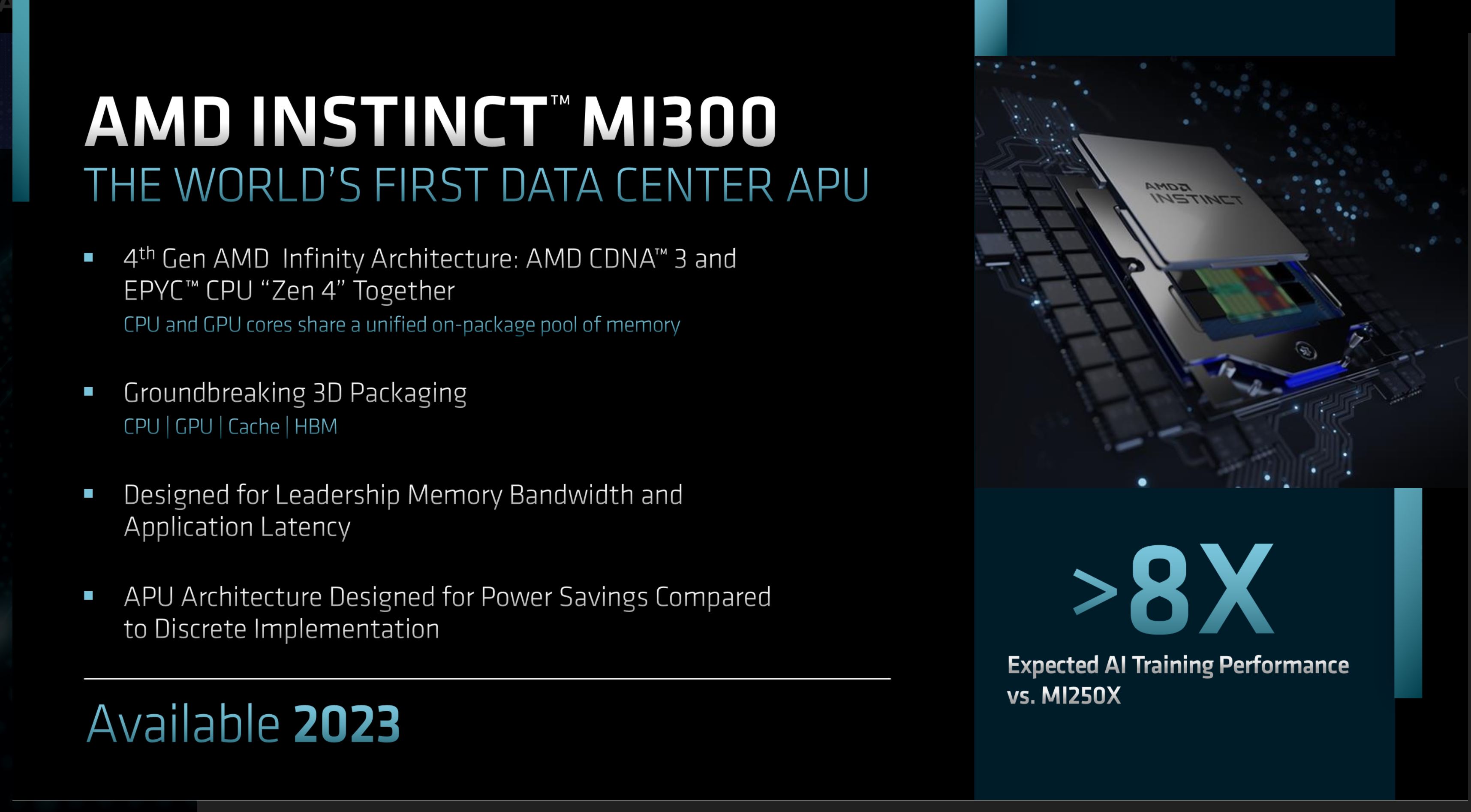
The reveal of the Instinct MI300 server APU was certainly the star of the Financial Analyst Day as far as immediate roadmap goes. David Wang, senior vice president of engineering for the Radeon Technologies Group at AMD, was positively buzzing as he revealed the CDNA 3 Unified Memory APU Architecture behind the chip, although he left the reveal of the chip itself to Forrest Norrod, senior vice president and general manager of the Data Center Solutions Group. Interestingly, after Raja Koduri burnt out and left for Intel in late 2017, David Wang rejoined AMD in early 2018, apparently to take on a three-generation roadmap to GPU leadership, put in place by AMD CEO Lisa Su to mimic their success with the “Zen” CPU roadmap. It seems he has done well!
https://ir.amd.com/news-events/financial-analyst-day
Presumably, as other sources have hinted, Instinct MI300 will be used in the 2+ exaflop El Capitan supercomputer set to arrive next year. It is great to see the Exascale Heterogenous Processor finally coming to fruition after a decade of research and development. I expect we will hear more about MI300 in additional supercomputer wins soon.
https://www.amd.com/en/products/exascale-era
https://wccftech.com/amd-exascale-heterogeneous-processor-eh…
Obviously, this thing will use the latest advanced packaging, and it will be very interesting to eventually see the details on how it is all put together — especially the Infinity Cache, I/O and interposer/bridges (a fan-out layer with Elevated Fanout Bridges will be used, I guess, similar to MI200).
I guess they may drop DDR support and instead use fat CXL 2.0 links with memory extension support (using CXL.memory and CXL.cache protocols). That will save a lot of board space, otherwise needed for DDR slots around the APU sockets. The APU boards can then be supplemented by EPYC CPU boards with lots of DDR RAM, or other memory extension devices.
https://www.rambus.com/blogs/compute-express-link/
I presume the Infinity Cache is an L4 cache, or perhaps a System Level Cache on the memory side of the memory controller, sitting below the GPU and CPU chiplets, and that the CPU chiplets will be ordinary “Zen 4” CCDs with the ability to stack L3 V-Cache chiplets on top. It will also be interesting to see whether AMD will be able to stack V-Cache higher than one layer in the “Zen 4” generation.
Some over at AnandTech Forums think moving the V-Cache below the CCD chiplets is a better idea. However, I suspect AMD will work on perfecting the current approach for a few generations yet. The current approach is advantageous due to the ability to ship chips with and without V-Cache, as well as add more layers. It hence allows for a lot of flexibility and risk reduction. They do however need to keep heat under control — but in that regard they seem to do great with clever design and their relentless focus on power-efficiency.
https://www.anandtech.com/show/17445/amd-combining-cdna-3-an…
https://images.anandtech.com/doci/17445/2022-06-09%2014_16_3…
https://images.anandtech.com/doci/17445/2022-06-09%2013_46_3…