Papermaster interview after the Genoa launch focused on process shrinks and packaging.
Mark Papermaster: … So for two Epyc generations, we kept the I/O die at 14 nanometers and at with the third we shrank it to 12 nanometers. But eventually what happens is that the technology matures, and the analog mixed signal efficiency is there, and, frankly, the cost goes down. So you get the performance, power, and cost to bring that technology over and drive ROI.
But as you know, that gets harder as you go forward because those memory elements and analog mixed signals are still not scaling to the degree they are scaling with logic circuits. So you will continue to see us leverage technology to move chiplets at the optimum pace. This is how it came together for the fourth generation, and it really all came together.
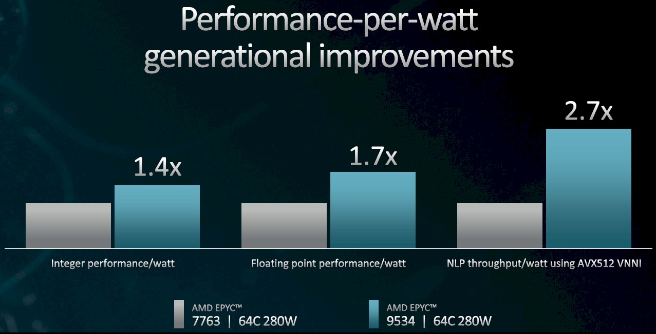
In this case, we had 5 nanometer process and design enhancements for the cores and with the I/O die we had a big technology change and the design optimization, too. From a performance per watt point of view, it is just a huge story. The specs I showed off at the launch tell the story: 1.4X on integer performance per watt, 1.7x on floating point performance per watt. And with AVX-512 support running BERT AI inferencing, we had 2.7X improvement generation to generation.
TPM: These are big jumps, core for core. You can’t do this every time, right?
Mark Papermaster: We are opportunistic, and at every transition, we’re going to pull every lever we can. And it’s not going to be consistent gen to gen. You’re just going to see different gains every gen. What our customers should do is look at the trend line and take an average on the dots and know that we’re going to be very aggressive gen over gen, always driving a gain in performance. Sometimes it’s a bigger IPC. Other times, it won’t be the IPC, it’ll be what we’re doing on throughput and overall total cost per core. So what we will do every generation is leverage the tools available, get the maximum customer benefit, and deliver it to them for what they care about.
TPM:
If the costs have flattened out and in some cases are going up, what do we do in a world where transistor costs – including design and manufacturing and yield – keep going up even as densities increase with 3 nanometer, 2 nanometer, 1.8 nanometer and so on? Are we going to depend – and I might say overdepend – on ever-better 2.5D and 3D packaging techniques and the use of chiplets to make up the difference so the performance of a socket goes up faster than its cost of manufacturing?
Mark Papermaster: Let me back up because you had a lot in there. I will make a few comments.
First of all, I said even in my comments at the 4th Gen Epyc launch in November, the key for us in maintaining a Moore’s Law pace is our chiplet approach. We believe that chiplets have been highly instrumental on keeping us on an accelerated performance growth, despite Moore’s Law. And the cost per transistor is going up. The cost piece of Moore’s Law is gone. You can’t stay in the same cost window while doubling the density of a chip every 18 to 24 months – that part is gone. But the exponential need for more density and performance at those generational paces, that’s actually still the same. So how do you do it?
So there is a new Moore’s law says you have to leverage a chiplet approach. …People realize that that is the right way to go, and you do this by effectively putting the circuits on the process node they want to be on. This is a big jump for Genoa. The CPU core went to 5 nanometer from 7 nanometer, but as I said, the I/O die went from 12 nanometer to 6 nanometer – and because it was the right time for both. The cost/performance trade off was there. But on the leading edge node, the cost per transistor is going up at each new leading edge because the jump itself is more costly and the mask counts keep going up at every turn. It’s an expensive value proposition.
TPM: How much does the process cost go up every time? Is it 5 percent? More? Less?
Mark Papermaster: I won’t give you a specific percentage there. But I have said publicly is gone is the day when you can increase the density such that your cost per transistor is flat – it is going up. And so what we do is we are leveraging process waves and making sure that we are really bringing the performance to stay on at a Moore’s Law pace. So what that does is it puts more pressure on the designers to not only bring IPC on the CPU engine, but it’s going to drive us to more and more heterogeneous computing and leveraging other accelerators. That’s how we’re going to stay at pace.
And how do you put all that together? It does require more packaging technology. And the trick is to keep that package technology highly yielding. And that’s what we are very focused on. So what we do is make sure we’re not using esoteric packaging.
If you look at the 4th Gen Epyc that we have today, it’s the same organic substrate that we had in Epyc generations one, two, and three. We have taken advantage of the manufacturing learnings over that time, but it’s not an esoteric technology. Yet, where you need other capabilities – take 3D V-Cache as an example – that uses a hybrid bonding technique and that does add cost and cycle time. But again, it’s not esoteric. We are an early pioneer with hybrid bonding, but we didn’t jump over to it until it was established and with good manufacturing yields.
So, it really is about the design choices, the power optimization choices, the foundry node choices, and the packaging choices that you make. And you have to make very, very careful tradeoffs between these when you do each generation.
You can stay on the Moore’s law curve of performance and density, but not the Moore’s law curve of cost per transistor.
…
TPM:* *Do you do the packaging and cooling? Do you create this expertise internally? Do you license things? Do you do fundamental research by yourself and also with the foundries?
Mark Papermaster: We have phenomenal expertise and packaging at AMD that got even much stronger yet again with the Xilinx acquisition because Xilinx was doing chiplets long before the acquisition. So, you know, it’s been a great partnership. And the way that we do it is deep partnerships with the foundries and the offshore test and assembly houses.
Let’s take hybrid bonding as an example. This is innovation from AMD paired with innovations from TSMC. And it results in a leading edge capability that goes out to the whole industry. We pioneer it, so we get early access, because we innovated with them. But we want to we want to see the cost come down. So we’re happy for it to be available to the industry. That’s the whole foundry model, right? An economy of scale. This is a beautiful aspect of our semiconductor ecosystem. It’s a global ecosystem and it works amazingly well to bring innovations into mass manufacturing.